
220nH RF Inductor 1608 | ABC ATEC Multilayer Chip
220nH, 250mA 1608 multilayer chip RF inductor for high frequency circuits. Compact design, -55°C to +125°C operating range. ABC ATEC quality certified.
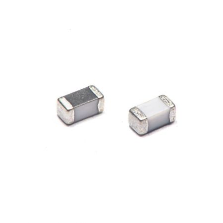
220nH, 250mA, 1608 RF Inductor, Multilayer Chip Inductor
MH1608R22JL
Multilayer Chip Inductor, General Grade
220nH, 250mA, 1608 Multilayer Chip Inductor MH series are compact, low-profile components with high self resonant frequency (SRF) and ceramic body can withstand operating temperature from -55°C to +125°C. They are well-suited for use in Smart phones, personal devices, high frequency circuits applications.
Product Features
- Multilayer structure
- Operating temp.: -55°C ~ +125°C (including self-temperature rise)
Product Applications
- Smart phones, personal devices
- High frequency circuits
| Product Category | RF Inductor - Multilayer Chip Inductor | Inductance (µH) | 0.22 |
| Part Number | MH1608R22JL | Tolerance | ±5% |
| Grade | General | RDC (Ω) | 2 |
| Length (mm) | 1.6 | IDC (A) | 0.25 |
| Width (mm) | 0.8 | Operating temp.°C (LOW) | -55 |
| Height (mm) | 0.8 | Operating temp.°C (HIGH) | 125 |
- Download

Multilayer Chip Inductor MH1608 Series Datasheet
Include dimensions, electrical characteristics and curve diagrams for your reference
Download- Related Products
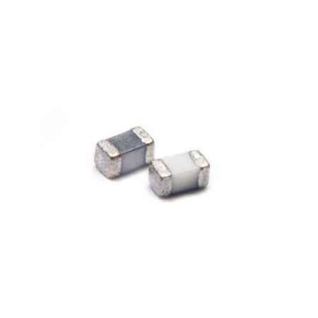
220nH, 100mA, 1005 RF Inductor, Multilayer Chip Inductor
MH1005R22JL
220nH, 100mA, 1005 Multilayer Chip Inductor MH series are compact, low-profile components with...
Details Add to List

 Download
 Hot Products

How can you source certified multilayer chip inductors that meet strict space and performance requirements for next-generation smartphone RF circuits?
ABC ATEC's MH1608R22JL multilayer chip RF inductor is specifically engineered for smartphone and personal device applications. With proven IATF16949 quality certification, high SRF performance, and compact 1.6mm × 0.8mm × 0.8mm dimensions, our inductor delivers the reliability and miniaturization your high-volume smartphone production demands. Our 45 years of inductor manufacturing expertise ensures consistent quality and technical support throughout your supply chain.
Engineered with ABC ATEC's 45 years of specialized expertise in inductor manufacturing and backed by IATF16949 quality certification, this multilayer chip inductor represents the convergence of miniaturization and reliability. The compact 1.6mm × 0.8mm × 0.8mm footprint maximizes PCB real estate efficiency without compromising electromagnetic performance, making it the ideal choice for OEM manufacturers and design engineers seeking certified, high-performance RF solutions. Contact ABC ATEC today to discuss customized inductor solutions tailored to your specific high-frequency application requirements and volume specifications.