
47nH RF Inductor | ABC ATEC Ceramic Wire Wound Chip
High-performance 47nH, 1000mA RF ceramic wire wound chip inductor with high Q factor and superior SRF. Ideal for cellular, ADSL, and Bluetooth applications.
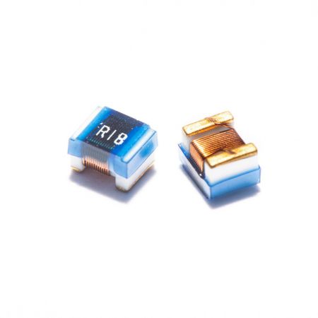
47nH, 1000mA, 1008 RF Inductor, Ceramic Wire Wound Chip Inductor
SWI1008CT47N
RF Ceramic Wire Wound Chip Inductor, General Grade
47nH, 1000mA, 1008 RF Ceramic Wire Wound Chip Inductor SWI CT series with minimum tolerance 2% available, advance in higher self resonate frequency (SRF), high Q factor, and is widely used in the co mmunication applications such as cellular phones, cable modem, ADSL, repeaters, Bluetooth, and other electronic devices.
Product Features
- Higher Self Resonate Frequency (SRF)
- High Q factor
- Tight tolerance ± 0.2nH and 2% available
- Operating temp.: -40°C ~ +125°C (including self-temperature rise)
Product Applications
- Metaverse application
- RF circuits
| Product Category | RF Inductor - Ceramic Wire Wound Chip Inductor | Inductance (µH) | 0.047 |
| Part Number | SWI1008CT47N | Tolerance | ±2% |
| Grade | General | RDC (Ω) | 0.1 |
| Length (mm) | 2.6 | IDC (A) | 1 |
| Width (mm) | 2.1 | Operating temp.°C (LOW) | -40 |
| Height (mm) | 1.7 | Operating temp.°C (HIGH) | 125 |
- Download

RF Ceramic Wire Wound Chip Inductor SWI1008CT Series Datasheet
Include dimensions, electrical characteristics and curve diagrams for your reference
Download- Related Products
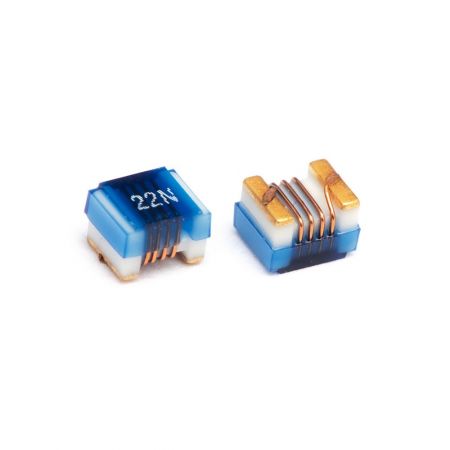
47nH, 1200mA, 1008 RF Inductor, Ceramic Wire Wound Chip Inductor
SWI1008HQ47N
47nH, 1200mA, 1008 RF Ceramic Wire Wound Chip Inductor SWI HQ series with minimum tolerance...
Details Add to List

 Download
 Hot Products

How can we optimize RF circuit performance while maintaining compact PCB layouts in next-generation communication equipment?
ABC ATEC's 47nH RF ceramic wire wound chip inductor delivers superior Q factor and self-resonant frequency performance in a compact 1008 form factor, enabling you to achieve optimal RF circuit efficiency without sacrificing board space. With tight tolerance control (±2%) and proven reliability across -40°C to +125°C operating range, this component is engineered for high-volume production of cellular, ADSL, and cable modem applications. Our 45 years of inductor manufacturing expertise and IATF16949 certification ensure consistent quality for your demanding RF applications.
Manufactured with ABC ATEC's 45 years of specialized inductor expertise and backed by IATF16949 Quality Certification, this RF inductor integrates seamlessly into next-generation communication systems requiring high-frequency performance and reliability. The compact 1008 form factor (2.6mm × 2.1mm × 1.7mm) with minimal DC resistance of 0.1Ω enables efficient space utilization in modern PCB designs. Whether designing cutting-edge RF circuits for telecommunications infrastructure, consumer electronics, or emerging metaverse technologies, ABC ATEC's ceramic wire wound chip inductor delivers the precision, quality, and performance specifications your applications demand. Contact our technical team today to explore customization options and volume pricing for your RF circuit integration projects.