
330nH, 650mA, 1210 RF Inductor, Ceramic Wire Wound Chip Inductor | Premier Manufacturer of High-Quality Power Inductors | ABC ATEC
330nH, 650mA, 1210 RF Ceramic Wire Wound Chip Inductor SWI CT series with minimum tolerance 2% available, advance in higher self resonate frequency (SRF), high Q factor, and is widely used in the co mmunication applications such as cellular phones, cable modem, ADSL, repeaters, Bluetooth, and other electronic devices. ABC ATEC is an efficient 330nH, 650mA, 1210 RF Inductor, Ceramic Wire Wound Chip Inductor, RF Ceramic Wire Wound Chip Inductor, General Grade, Chip inductor, Power inductor, Common Mode Choke, RF Inductor, Transformer, ConnectorChip inductor, Power inductor, Common Mode Choke, RF Inductor, Transformer, Connector manufacturer. With 45 years of expertise in professional inductor design and manufacturing, we offer tailored services for inductors, transformers, connector, thermal solutions, and mechanical partts. Our solutions cater to various sectors including automotive, industry, telecommunications, medical and consumer electronics applications. We are proud to have achieved IATF16949 Quality Certification, ensuring the highest standards in our products. Additionally, we continuously innovate, holding key production technologies and patents to enhance our offerings.
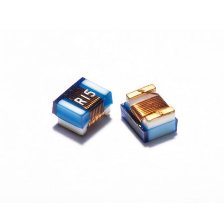
330nH, 650mA, 1210 RF Inductor, Ceramic Wire Wound Chip Inductor
SWI1210CTR33
RF Ceramic Wire Wound Chip Inductor, General Grade
330nH, 650mA, 1210 RF Ceramic Wire Wound Chip Inductor SWI CT series with minimum tolerance 2% available, advance in higher self resonate frequency (SRF), high Q factor, and is widely used in the co mmunication applications such as cellular phones, cable modem, ADSL, repeaters, Bluetooth, and other electronic devices.
Product Features
- Higher Self Resonate Frequency (SRF)
- High Q factor
- Tight tolerance ± 0.2nH and 2% available
- Operating temp.: -40°C ~ +125°C (including self-temperature rise)
Product Applications
- Metaverse application
- RF circuits
| Product Category | RF Inductor - Ceramic Wire Wound Chip Inductor | Inductance (µH) | 0.33 |
| Part Number | SWI1210CTR33 | Tolerance | ±2% |
| Grade | General | RDC (Ω) | 0.37 |
| Length (mm) | 3.2 | IDC (A) | 0.65 |
| Width (mm) | 2.6 | Operating temp.°C (LOW) | -40 |
| Height (mm) | 2.1 | Operating temp.°C (HIGH) | 125 |
- Download

RF Ceramic Wire Wound Chip Inductor SWI1210CT Series Datasheet
Include dimensions, electrical characteristics and curve diagrams for your reference
Download

 Download
 Hot Products

330nH, 650mA, 1210 RF Inductor, Ceramic Wire Wound Chip Inductor | High-Efficiency Chip Inductors for Automotive Electronics | ABC ATEC
ABC ATEC, established in 1979 and headquarter in Yangmei, Taiwan, is a premier manufacturer of high-quality inductors. Our extensive product range includes 330nH, 650mA, 1210 RF Inductor, Ceramic Wire Wound Chip Inductor, chokes, filters, chip inductors, power inductors, common chokes, and RF inductors. With more than four decades of experience in the industry, we have developed and possess key production technologies and numerous patents, positioning us at the forefront of innovation and quality in inductor manufacturing.
With 45 years of expertise in professional inductor design and manufacturing, we offer tailored services for inductors, transformers, connector, thermal solutions, and mechanical partts. Our solutions cater to various sectors including automotive, industry, telecommunications, medical and consumer electronics applications. We are proud to have achieved IATF16949 Quality Certification, ensuring the highest standards in our products. Additionally, we continuously innovate, holding key production technologies and patents to enhance our offerings.
ABC ATEC has been offering customers efficient power inductors since 1979. With both advanced technology and 45 years of experience, ABC ATEC always ensures to meet each customer's demands.